

Related posts
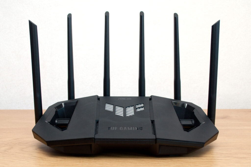
The WiFi Router Guide (2026): What the Labels Mean, What to Buy, and the Five-Minute Fixes
body.postid-270075{--font:system-ui,-apple-system,'Segoe UI',Roboto,'Helvetica Neue',Arial,sans-serif;--ink:#1...
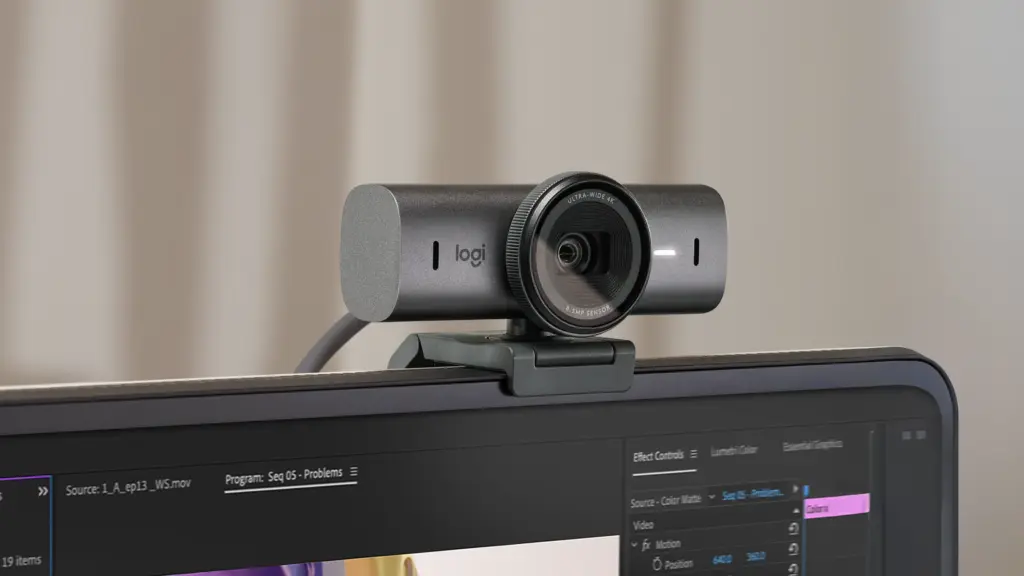
Best Webcams in 2026: For Zoom, Streaming, Tight Budgets and Everything Else
body.postid-270062{--font:system-ui,-apple-system,'Segoe UI',Roboto,'Helvetica Neue',Arial,sans-serif;--ink:#1...
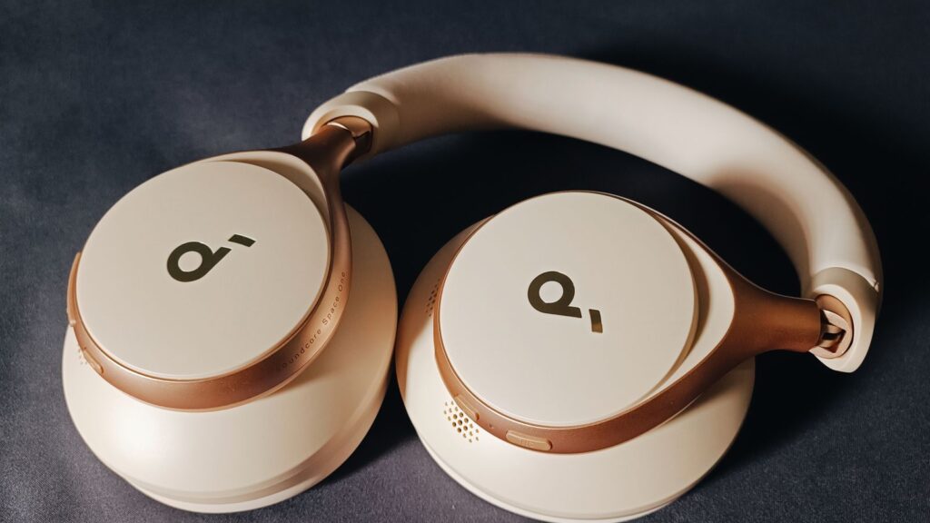
Best Noise Cancelling Headphones in 2026: Real Picks, How It Works, and the Truth About Your Ears
body.postid-270035{--font:system-ui,-apple-system,'Segoe UI',Roboto,'Helvetica Neue',Arial,sans-serif;--ink:#1...
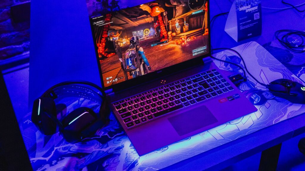
Best Gaming Laptop in 2026: The Right Pick at Every Budget, and the Traps to Avoid
body.postid-269923{--font:system-ui,-apple-system,'Segoe UI',Roboto,'Helvetica Neue',Arial,sans-serif;--ink:#1...
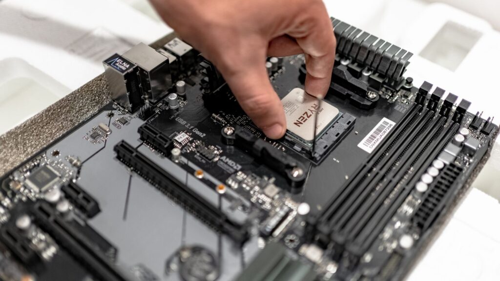
How to Build a PC in 2026: Step by Step, With the Problems Nobody Warns You About
body.postid-269917{--font:system-ui,-apple-system,'Segoe UI',Roboto,'Helvetica Neue',Arial,sans-serif;--ink:#1...
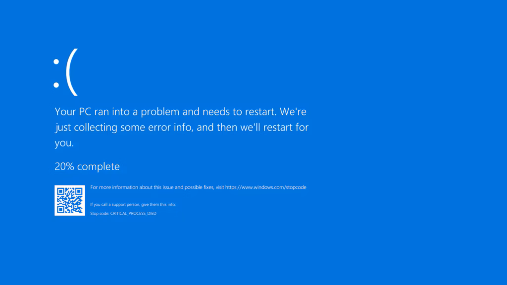
Blue Screen of Death: The Complete 2026 Fix Guide (Every Stop Code, Every Real Fix)
body.postid-269868{--font:system-ui,-apple-system,'Segoe UI',Roboto,'Helvetica Neue',Arial,sans-serif;--ink:#1...

Are Gaming Chairs Bad for Your Back? The Honest Truth (and What to Buy Instead)
Are gaming chairs bad for your back? The honest answer: not automatically, but cheap racing-bucket chairs often are over long hours. Here is what actually protects your spine, how gaming chairs compare to ergonomic office chairs, and what to look for before you buy.
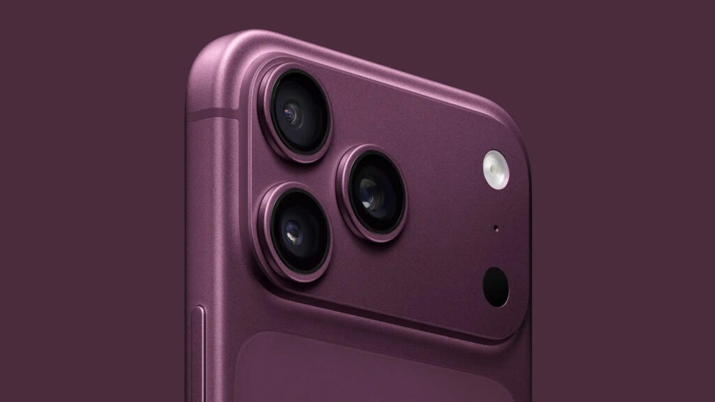
iPhone 18 Release Date: When Apple’s 2026 iPhones Land (and Should You Wait?)
When is the iPhone 18 coming out? Apple is splitting the launch: the iPhone 18 Pro, Pro Max and first foldable arrive September 2026, while the standard iPhone 18 waits until spring 2027. Full release dates, price, colours, charger and whether to wait or buy now.
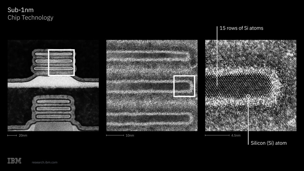
IBM Built the World’s First Sub-1nm Chip: What 0.7nm ‘Nanostack’ Really Means
IBM has unveiled the world's first sub-1-nanometre chip, a 0.7nm node built with a new 3D nanostack architecture. Here is what it really means, why the number is not a measurement, and how far it is from your PC.
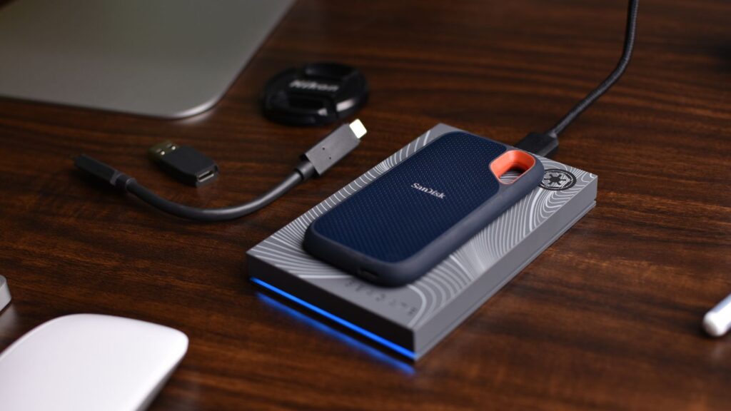
The Stutter That Isn’t Your GPU: How Game Downloads Throttle Your SSD
A game download is one of the heaviest jobs you can give an SSD. It fills the drive's fast cache and heats the controller, so the whole PC stutters and you blame the GPU. Here is what is really happening and how to fix it.
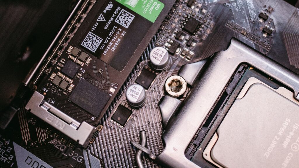
SSD Not Detected? The Complete 2026 Fix Guide (New Drive, NVMe and SATA)
body.postid-269306{--font:system-ui,-apple-system,'Segoe UI',Roboto,'Helvetica Neue',Arial,sans-serif;--ink:#1...
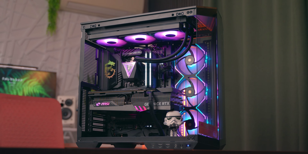
Buying a Gaming PC in 2026: How Much to Spend, What to Avoid, and the Mistakes We See Every Week
How much to spend on a gaming PC in 2026, what to avoid, and the mistakes we see every week. An honest UK buying guide from the Hardvance bench.